Setbacks and Prospects for Autonomous Vehicles
By Henry Petroski
Self-driving cars seemed ready to keep going ahead, but some recent incidents have slowed their development.
Self-driving cars seemed ready to keep going ahead, but some recent incidents have slowed their development.

DOI: 10.1511/2017.124.27
In 2015, the future of self-driving, or autonomous, vehicles looked bright and virtually within reach. I described their status in The Road Ahead (July–August 2016), an excerpt from my 2016 book The Road Taken: The History and Future of America’s Infrastructure, as of the time the book had gone to press in the fall of 2015. Earlier that year a computer-controlled Audi Q5 successfully made a 3,400-mile trip from San Francisco to New York City without human intervention for 99 percent of the time. And Tesla’s all-electric self-steering and self-braking Model S sedan was coming onto the market. The road ahead for the autonomous vehicle looked smooth, indeed.
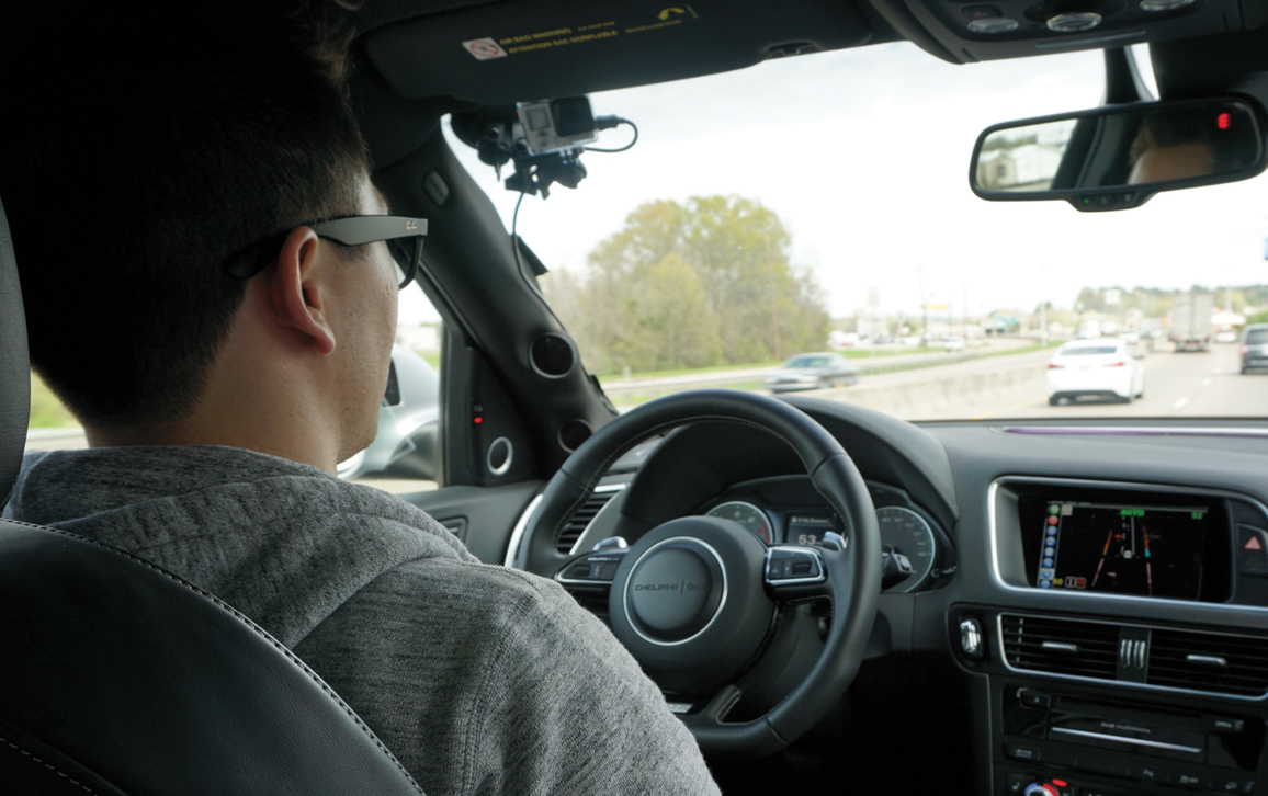
Delphi Automotive.
Click "American Scientist" to access home page

American Scientist Comments and Discussion
To discuss our articles or comment on them, please share them and tag American Scientist on social media platforms. Here are links to our profiles on Twitter, Facebook, and LinkedIn.
If we re-share your post, we will moderate comments/discussion following our comments policy.